



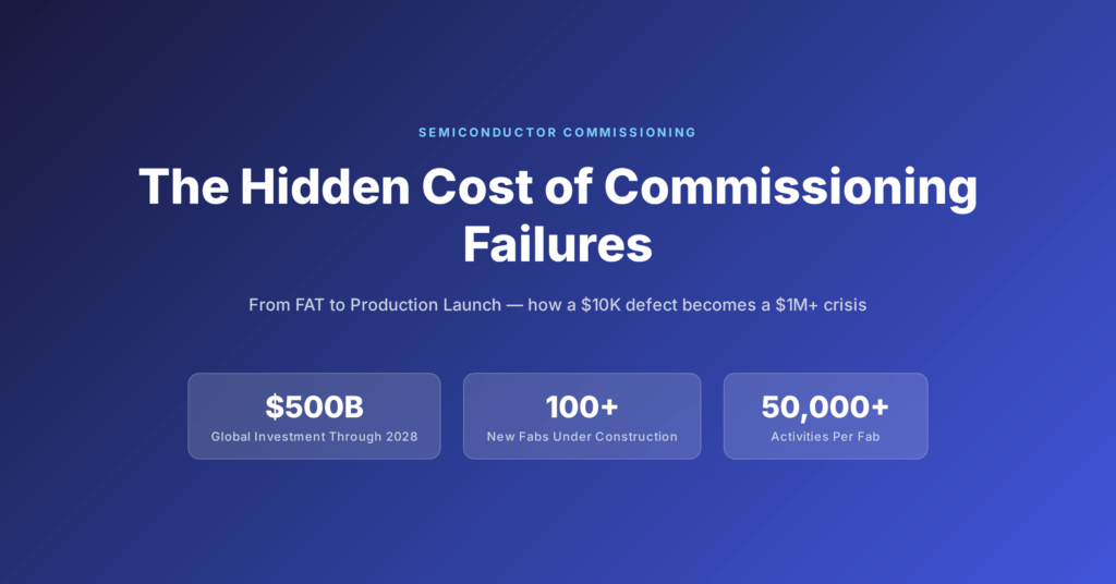
The semiconductor manufacturing renaissance is real. The CHIPS Act. Geopolitical supply chain resilience. AI chip demand. Investment is unprecedented: $500 billion globally through 2028 (source: SEMI World Fab Forecast, 2025), with 100+ new fabs either under construction or ramping production in the next 36 months.
This expansion is colliding with a brutal reality: the teams that know how to execute high-volume semiconductor commissioning at scale have never been more valuable—or more overloaded.
And for every fab that’s winning the commissioning race, another is discovering the same lesson learned by semiconductor leaders over the past decade: a single commissioning failure doesn’t just cost money. It cascades.
The Semiconductor Commissioning Sequence
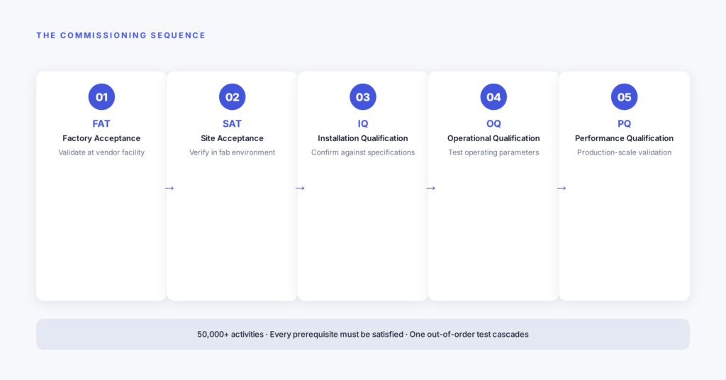
A semiconductor fab is a precision manufacturing environment. Every system—chemical delivery, ultra-pure water, photolithography, clean room pressure, thermal control, electrical distribution—must work together within micron-level tolerances. Commissioning happens in stages:
- FAT (Factory Acceptance Test): Equipment validated in the manufacturer’s facility before shipment.
- SAT (Site Acceptance Test): Equipment tested in the actual fab environment for real-world performance.
- IQ (Installation Qualification): Installation verified against specifications—connections, positioning, utility isolation.
- OQ (Operational Qualification): Systems operated at normal parameters; safety interlocks and alarms validated.
- PQ (Performance Qualification): Continuous production-scale operation to verify sustained quality output.
On a modern semiconductor fab project, commissioning can involve tens of thousands of inspections, tests, approvals, and dependencies across hundreds of systems. Every prerequisite dependency must be satisfied. One out-of-order test can invalidate entire test sequences downstream.
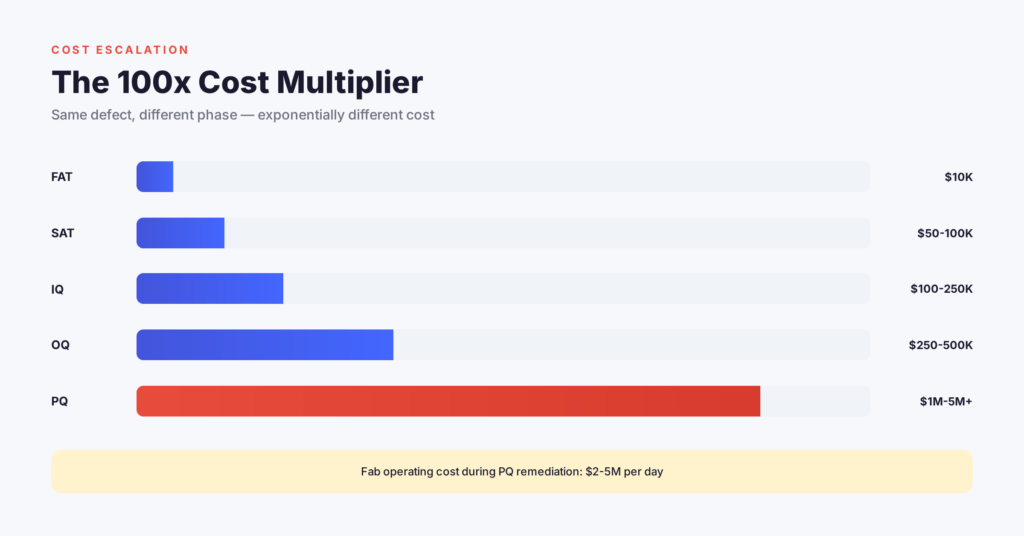
The cost escalation is sharp:
| Phase | Remediation Cost | Impact |
|---|---|---|
| FAT | ~$10,000 | Manufacturer corrects, equipment ships on schedule |
| SAT | $50K–$100K | On-site troubleshooting, manufacturer specialists, partial reinstallation |
| IQ | $100K–$250K | Facility downtime, blocked downstream activities, idle contractors |
| OQ | $250K–$500K | Equipment mothballing, compressed rework timelines, premium repair rates |
| PQ | $1M–$5M+ | Full operating cost exposure ($2–5M/day), customer allocation at risk, warranty disputes |
At this scale, commissioning becomes a data management challenge as much as an engineering one. Teams need visibility into dependencies, test status, documentation, and issue resolution across thousands of activities.
Why Traditional Commissioning Methods Fail at Semiconductor Complexity
Semiconductor fabs represent the highest complexity commissioning environment in industrial manufacturing. Here’s why traditional methods break down:
Extreme System Interdependence
A photolithography track cannot run until the chemical delivery system is validated. Chemical delivery cannot run until the ultra-pure water loop passes pressure tests. The water loop cannot be certified until the chiller demonstrates 72-hour thermal stability. One failed prerequisite creates a chain reaction of blocked activities. Traditional paper-based commissioning has no mechanism to enforce these prerequisites or prevent contractors from attempting tests with unmet dependencies.
International Equipment Vendor Coordination
A typical advanced fab involves equipment from 20–40 vendors: ASML, Applied Materials, LAM, KLA, Tokyo Electron, Entegris, and more. Coordination across language barriers, time zones, and organizational boundaries breaks down with email and spreadsheets. When issues arise, root cause investigation becomes impossible—who was responsible for that test? When did it fail? Were specifications updated after commissioning started?
ng used at the time? Were they updated after commissioning started?
Regulatory and Compliance Complexity
Semiconductor fabs operate under strict EPA, OSHA, and international environmental regulations. Commissioning documentation isn’t just useful—it’s legally required. You must prove hazardous chemical handling and wastewater treatment systems were properly tested and validated. Paper logs and fragmented spreadsheets don’t create auditable records. When an EPA inspector arrives six months into operations asking for proof, you can’t produce it. You’re looking at fines or facility shutdowns.
The takeaway: in semiconductor commissioning, catching a defect at FAT versus IQ isn’t a budget question — it’s the difference between hitting a market window and watching a competitor take it. Digital commissioning doesn’t remove the complexity of a fab startup, but it gives every stakeholder the visibility, traceability, and prerequisite enforcement to keep small issues small. That’s how the manufacturers we work with are reducing FAT errors by 75% and shaving 30 days off their commissioning schedules.
Ready to Accelerate Your Semiconductor Commissioning?
If you’re planning or managing semiconductor fab commissioning, expansion, or process ramp, we’d like to show you how digital commissioning can prevent the 100x cost escalation that happens when defects escape from FAT into later phases.
Exto’s zero-trust multi-enterprise architecture was built for exactly this challenge. If your commissioning project involves multiple contractors and you’re still coordinating with spreadsheets and status meetings, schedule a call to see how Exto can bring order to the chaos.